
Creating a A-Stable 555 Timer Circuit using the NE555 Precision Timer
Hello, And today I'll show you how to assemble, read, and analyze the signal created via the 555 Timer Circuit using a NE555 IC, ( Integrated Circuit), on a Breadboard. In this tutorial we'll be using the NE555 model timer. Most Precision Integrated Timer Circuits, ( Like the standard HA17555, or HA17555S, Series Circuit ) will work fine for this case since they both work with building both A-stable, and Mono-stable Circuit Configurations.
But do keep in mind that for the process of wiring, and hooking up the circuit will be different depending on what certain model of IC, (Integrated Circuit) you're using.
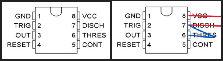
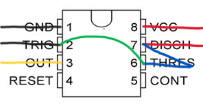
*Check your 555 timer's datasheet for more information on the chip's pin-out diagram*
Setting up the circuit:
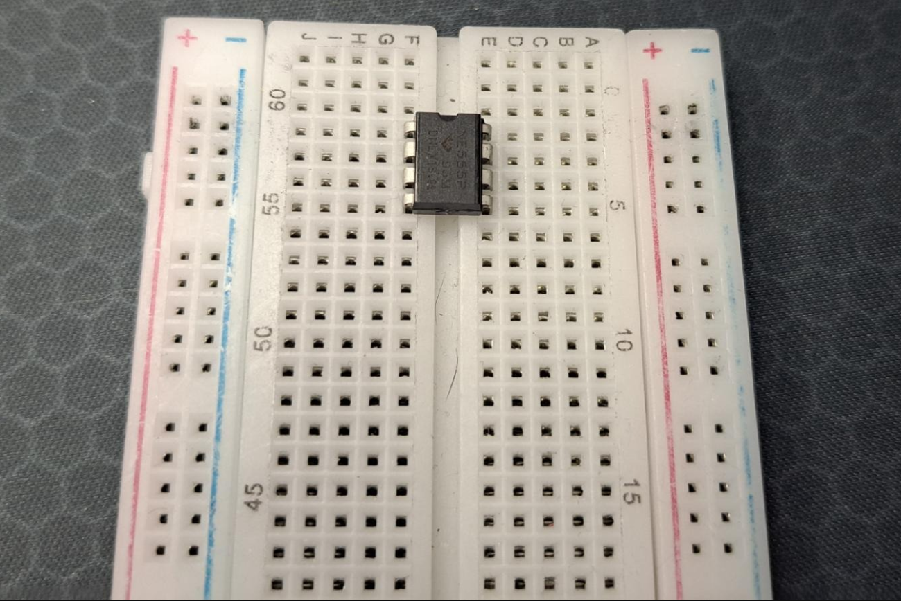
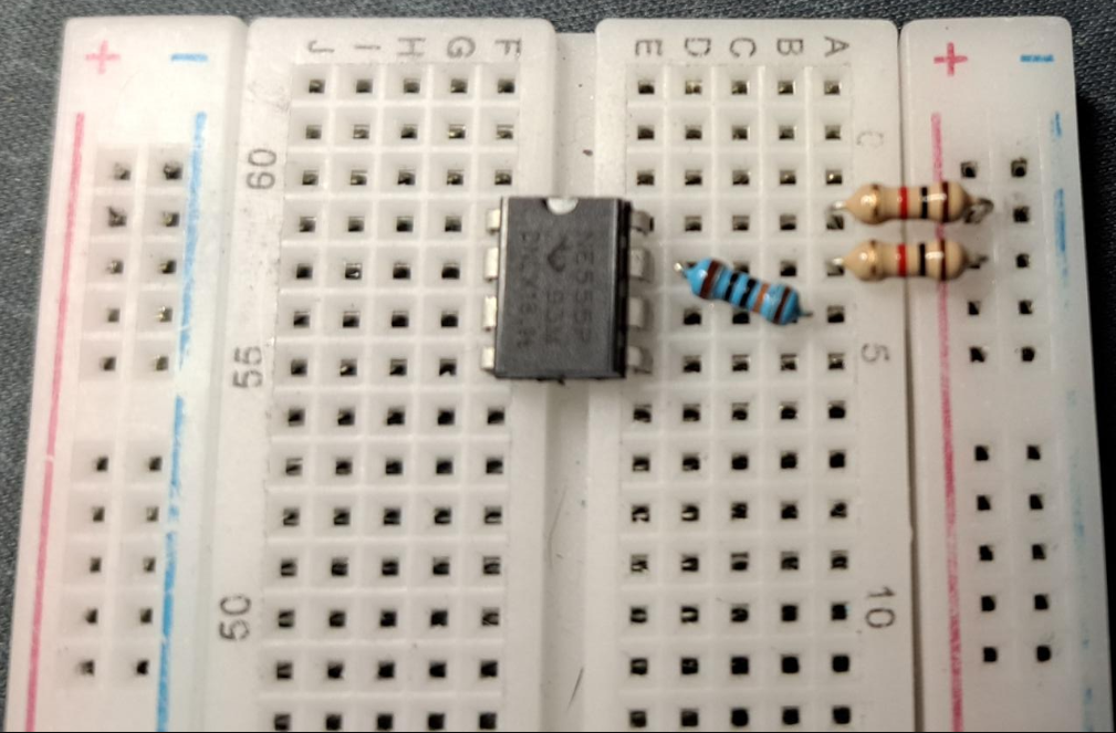
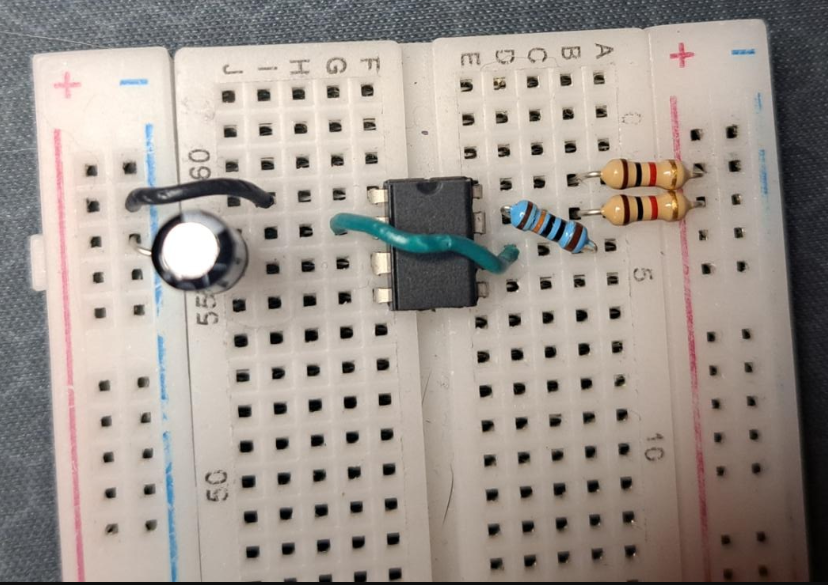
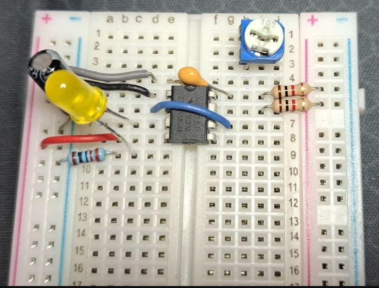
Firstly go ahead and attach your 555 Timer directly to the breadboard. Make sure to place the IC in the center gap of the board, bridging the two sides as shown in the picture below.
Figure 1
Generally for using a standard 555 Timer Circuit like the, "HA17555", or, "HA17555S", you'll want to connect Pin 6 of the 555 Timer to the + 5 Volt Powerline on your Breadboard.
Figure 2
But for this case, since I'll be using the NE555 Integrated Circuit for my timer, we'll have to look at this section of the data sheet that lists the following about using the NE555 Circuit for A-Stable, & Mono-Stable mode timers:
"As shown in Figure 12, adding a second resistor, ( RB ), to the circuit of Figure 9 and connecting the trigger input to the threshold input causes the timer to self-trigger and run as a multi-vibrator. The capacitor ( C ) charges through ( RA ) and ( RS ) and then discharges through ( RS ) only. Therefore the duty cycle is controlled by the values of ( RA ), and ( RB ).
This astable connection results in capacitor ( C ), charging and discharging between the threshold-voltage level (≈
0.67 × VCC) and the trigger-voltage level (≈ 0.33 × VCC). As in the mono-stable circuit, charge and discharge times (and, therefore, the frequency and duty cycle) are independent of the supply voltage."
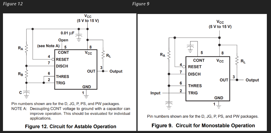
This means for our use case here, adding that additional 1k resistor, ( RB ), will allow the capacitor ( C )'s. charge and discharge rate to be between the threshold-voltage level (≈ 0.67 × VCC) and the trigger-voltage level (≈ 0.33 × VCC). Note Mono-stable operations requires wiring the resistor ( RB ), and the 0.01 uF capacitor on the +5 Vcc line
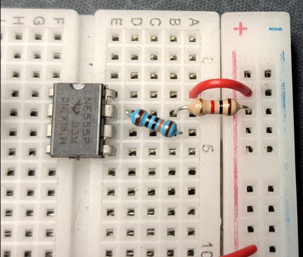
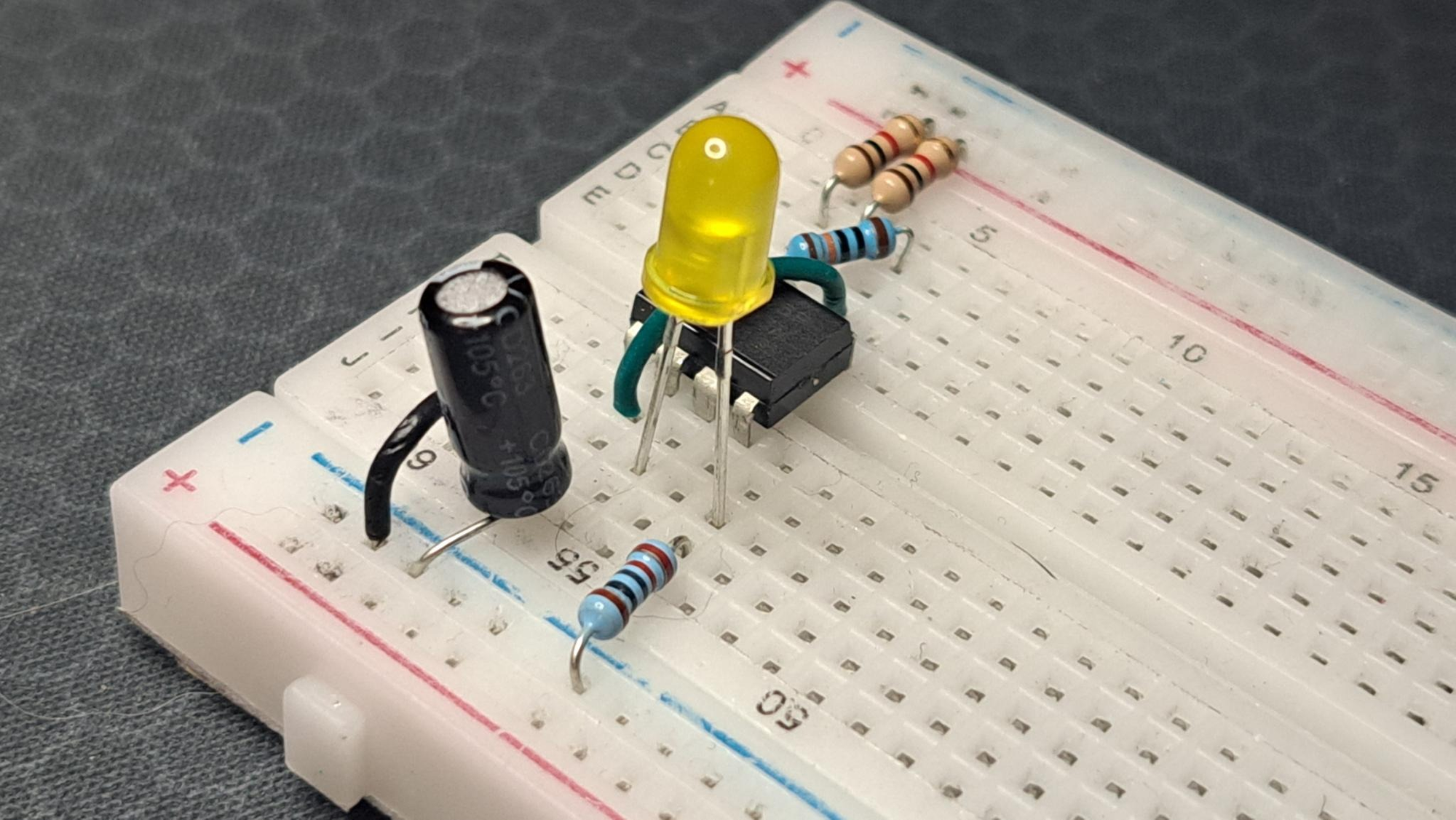
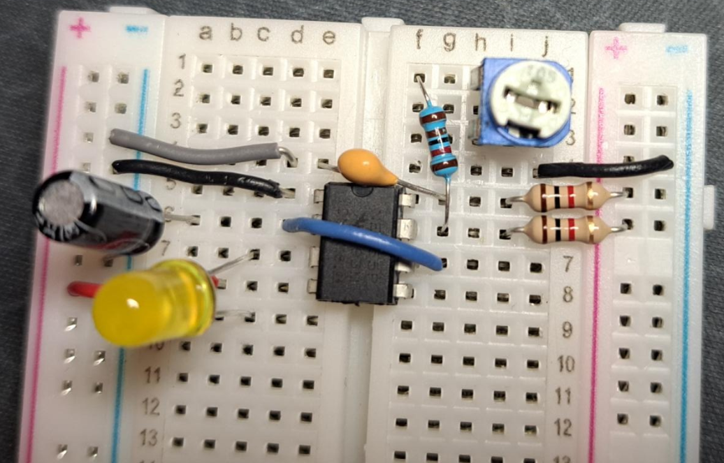
So in the case you're using a NE555 Timer, go ahead and attach a 1k Ohm resistor from the 5 Volt power supply on your Breadboard, to Pin 8 on the chip through a 1k Ohm resistor. ( Fig 3 ).
Figure 3
**Pin-Out Diagram below for more info**
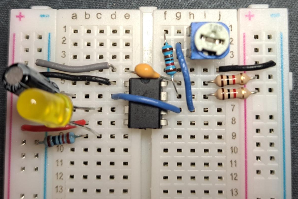
Place a (1uf) micro-farad Capacitor into Pin 2 (TRIGGER) of the Chip, and a wire connection (Black Wire), from the 555 Timer's Pin 1 to the Ground Line. (Figure 4 below)
Figure 4
Make sure that your capacitors orientation is in the correct position. The Grey strip should be facing towards the right, with the Anode (Long Leg), inserted into the Ground line of your Breadboard.
*Note: Improper placement/wiring may result in capacitors exploding at high Voltages*
Then, Go ahead and place a wire connection, (Green Wire) from Pin 6 (TRIGGER), onto Pin 2 of the Chip. This will provide the capacitor with power to fill up with through the 100k Ohm resistor we attached Pin 6. ( Figure 5 Below )
Figure 5
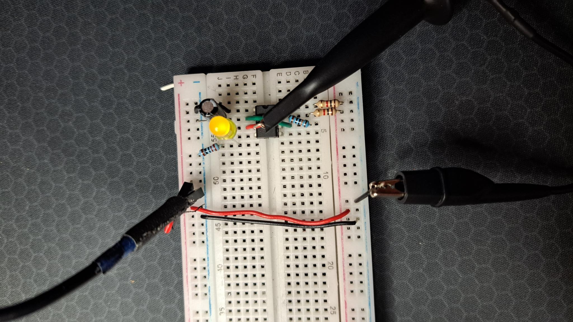
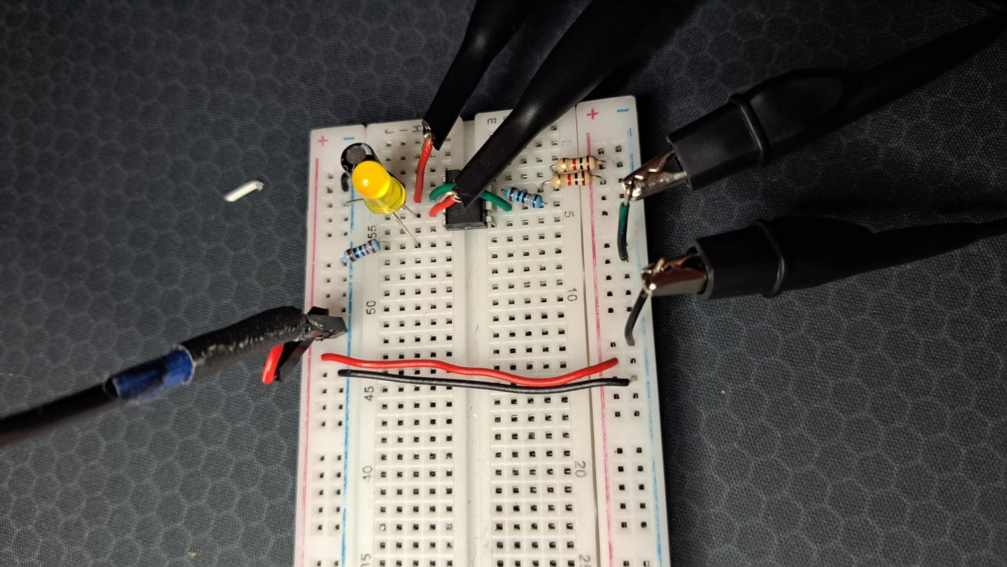
The output signal of the 555 Timer is on Pin 3 of the Chip. Place an LED with the Anode side, (Longer Leg), in the same line as Pin 3. And Cathode side (Shorter Leg), to Ground through a 220 Ohm Resistor. (See Figure 6)
Figure 6
Powering on the Circuit
Now lets move onto actually powering on the 555 Timer Circuit.
Plug in you Power and Grounds lines to a 5 Volt, power supply. For my case I'll be using an old USB cable that I've crimped and soldered the ends off to plug straight into the Breadboard.
When powering on the circuit you should end up seeing the LED start Blinking ON and OFF.
*If the LED does not just start Blinking or is just ON, you may have to check the Resistors, /and or, Capacitor Values for proper timing adjustment*
Figure 7
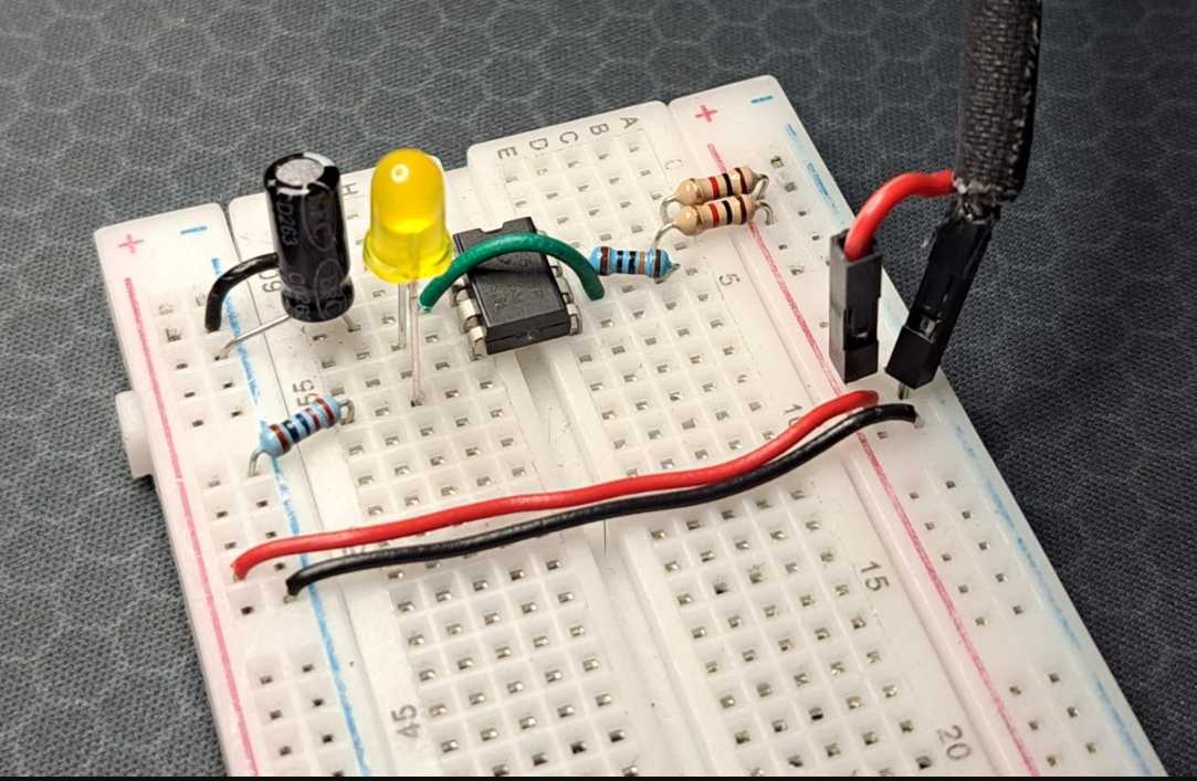
The Ground and Power of my Breadboard are connected together so that both sides of the Circuit shares the same PWR & GND lines.
Measuring & Reading the Signal coming from the 555 Timer
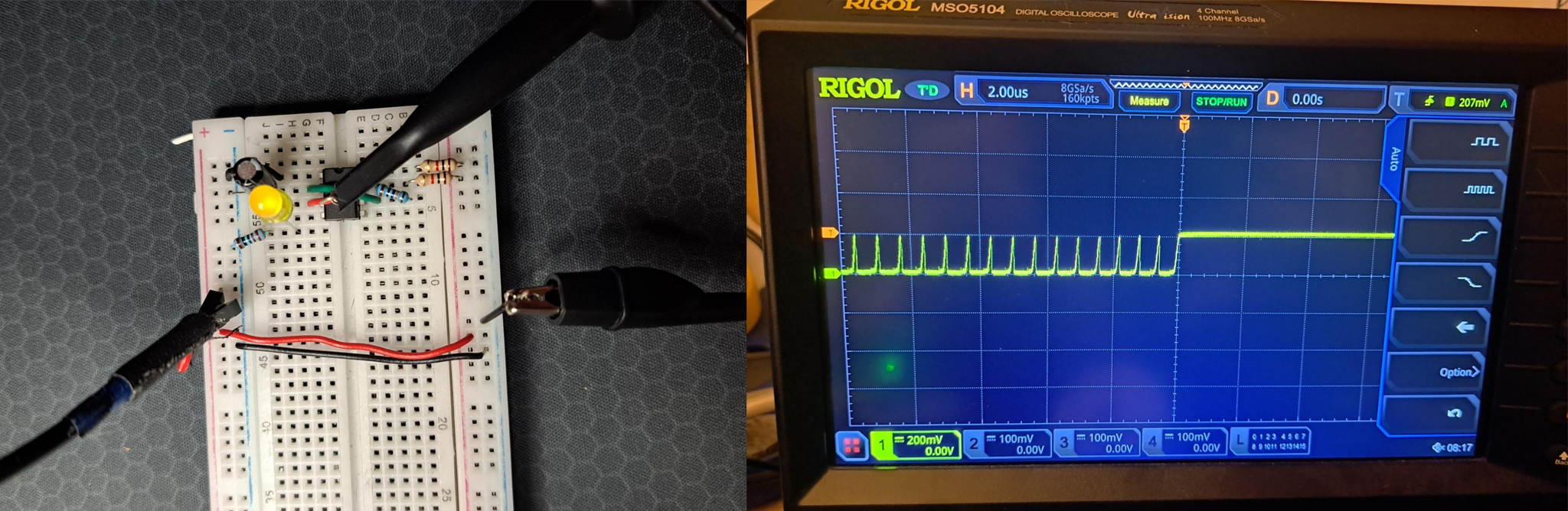
So now, let's move onto reading the signal being produced by the 555 Timer Circuit, using a Probe connected to an Oscilloscope.
Start by attaching a couple of wires to both arms of the probe using the clips at each end, ( * Or any probes that work with your brand of Oscilloscope *)
Connect the one end of the probe to the Ground line on your breadboard, and the other to Pin 3 on the timer, ( The output pin. ), the same line the LED's Anode side, is plugged into, (The Longer Leg ).
Figure 8
You'll have to adjust the various settings depending on your brand Oscilloscope to make sure that the scale of the sign-wave is correct and should look something like shown in the picture below:
Figure 9
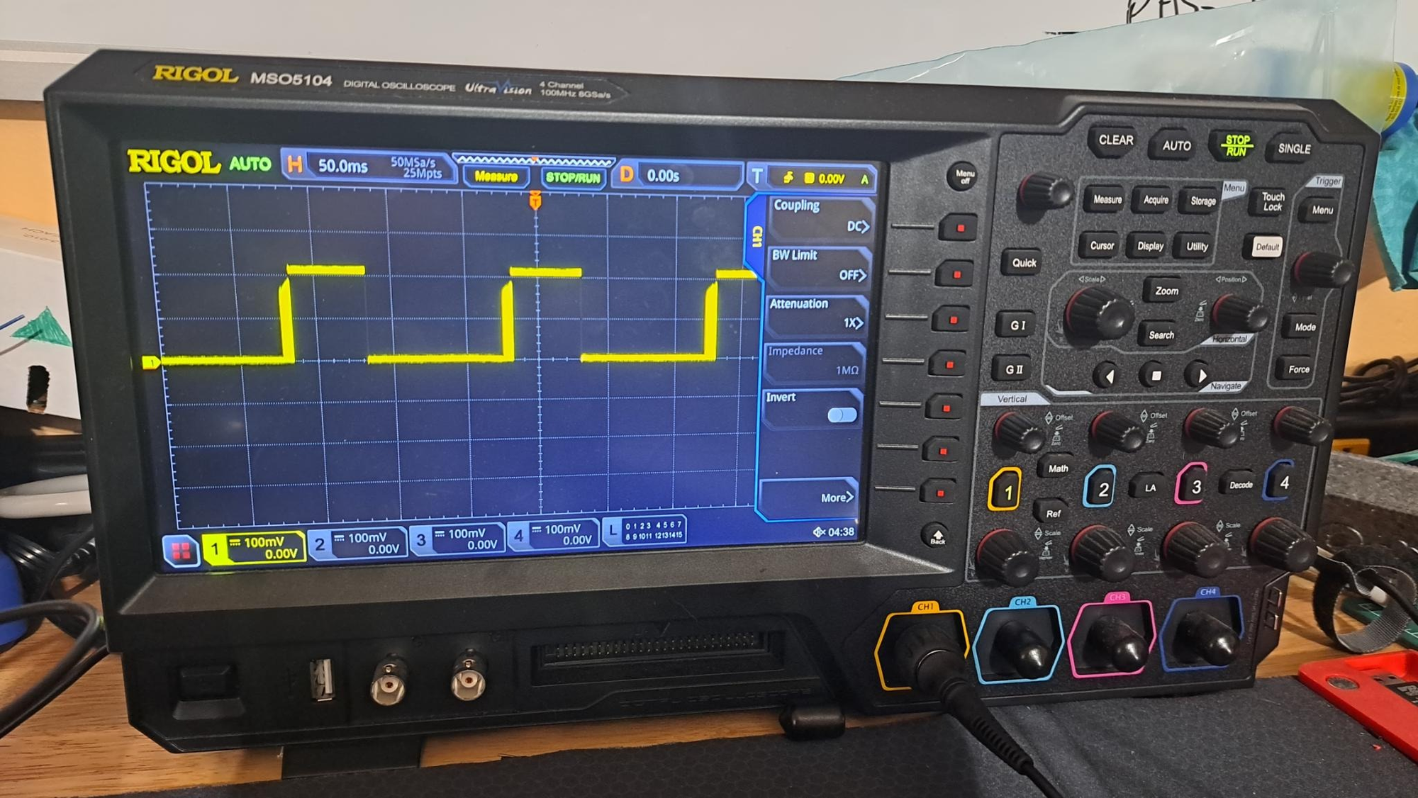
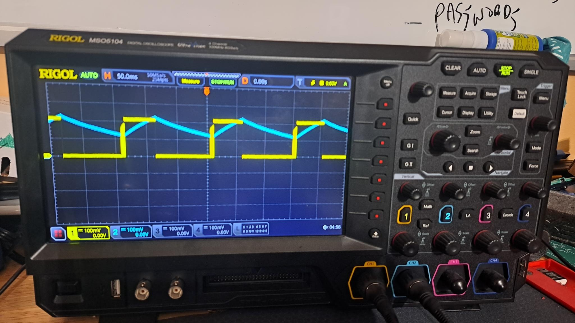
The Yellow line on the picture shown above is the output signal we created, on Pin 3 of the 555 Timer. You should be able to see the signal move up and down as the LED on your breadboard flashes On and Off.
Here we see the 50.0ms (milli-second), signal we're reading from the oscilloscope's Probe. Its in the 100mV (milli-Volt) range, with the bottom of the yellow, line, our output voltage at, (0.00) Volts on the bottom, and about (3.00 something) Volts on the top.
*note the volts on your meter may also hover around 3.00 to 4.00-ish Volts. This is perfectly normal as stated in the Data Sheet for the NE555 Timer, "Minimum Output Voltage as = 3.33 Volts", and we see something around that on our Oscilloscope in the picture below*
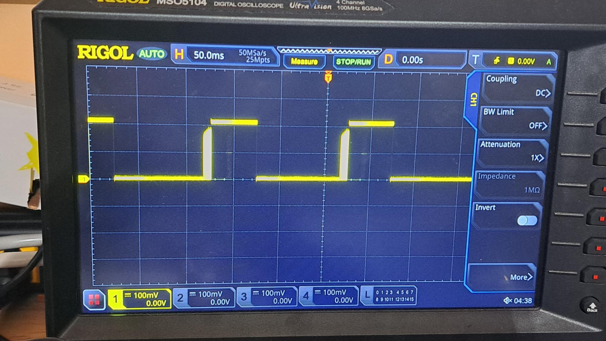
Figure 10
Now let's take a step back for a second to understand exactly what is happening inside the 555 Timer.
Inside of the 555 Timer.
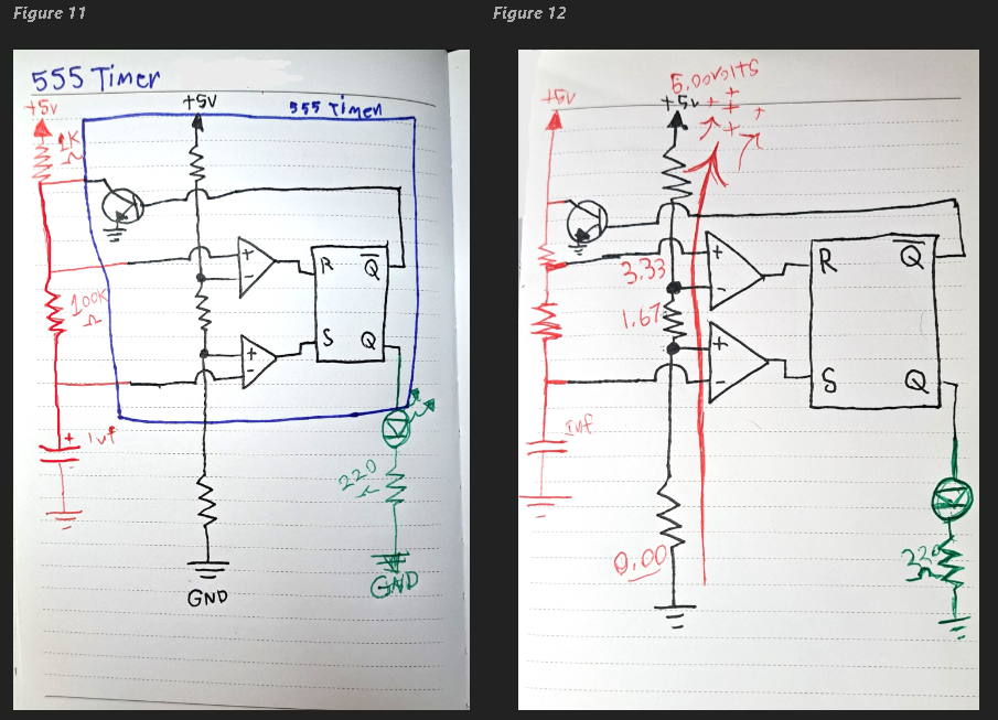
Below we see a drawing of the 'Block Diagram' for the 555 Timer Circuit. (Figures 11 &, 12), ( * As provided by Ben Eater, Links to his project used for certain references throughout this walkthrough: https://eater.net/ *)
In this Diagram, ( Figures 11, & 12 ), we see two main things, an SR-Latch, and a pair of comparators. Everything we see inside the blue box on the left is everything inside the 555 Timer.
The Black Power line running through the center of the 555 timer is a form of Voltage divider. That divider has three, 5k (Kilo- Ohm) resistors running along the 5 Volt power line on the inside of the 555 timer. In turn, splitting the Voltage into thirds from 5.00 Volts, down to 3.00 Volts, then subsequently 1.67 Volts, and finally to Ground, 0.00 Volts. ( See Figure 12 for more info )
The SR-Latch is a component that, in it of itself, is a little complicated and I can't quite go into full detail in this tutorial, but basically its function works something like this:
An SR-Latch has two input Terminals, and two output Terminals, a Set, ( S ), a Reset ( R ), an Output ( Q ), and an Inverse Output ( Q' ).
The Set ( S ), in the SR-Latch sets the Output ( Q ), voltage HIGH when the Set ( S ) comparator connected to the terminal is switched ON, letting current through.
The Reset ( R ), Terminal sets the Output ( Q ), voltage LOW, when the comparator connected to the Reset ( R ), is switched ON, turning OFF the Set ( S ) terminal.
The Inverse Output ( Q' ), in the SR-Latch is just always the opposite of ( Q ), Output. In the schematic shown below, the Inverse Q inside this circuit is leading to a Discharge Transistor inside of the 555 Timer, going straight to ground.
The two comparators, in this circuit act as switches for both the Set ( S ), and the Reset ( R ), terminals on the SR-Latch.
Those comparators take in two input signals and compares the two. Letting only the higher voltage though. So with that in mind, taking a look back at the Schematic shown below, ( Figures 11, & 12 ), again we can see that the Comparators are running along the +5 Volt, Voltage divider. The bottom comparator ( Set ( S ), is between the third resistor and Ground of the Circuit. This means that the "+" Positive, side of the bottom comparator will be charged at 1.67 Volts, and the "-" Negative, at 0.00/Ground. This will turn on the comparator, in turn, turning on the Set ( S ) Terminal, powering on the Output ( O ) Terminal, HIGH.
Some thing to keep in mind, is that the Red line is the +5 Volt powerline coming from the Breadboard, down to the 1uF ( Micro-Farad ), capacitor. As that capacitor begins to charge, the voltage on the capacitor will rise, making the voltage along the Black voltage divider to also subsequently begin rising. This means, ( as shown in Figure 12 below ) that once the current goes above the second 5 Kilo-Ohm resistor along the voltage divider, changing the total voltage on that resistor 3.33 Volts. Since 3.33 is > than 5.00 Volts, the Reset ( R ), comparator latches ON, Turning OFF the Set ( S ) terminal, and making the Output ( O ), voltage LOW.
But something else also happens after the Reset ( R ), latch turns ON. The Inverse Output ( Q ), terminal also turns on, pulling the voltage down to that Pull-Down Resistor to Ground. This will start draining the 1uF Capacitor, lowering the voltage on the divider back down to 0, in turn, switching the Reset ( R ), latch OFF and the Set ( S ), back on. ( Since the average voltage along the voltage divider next to the second comparator is 1.67 Volts above, and 0.00/Ground below, the Set ( S ), comparator turns back on, starting the cycle over again. )
This process is how the 555 Timer circuit functions in generating an A-Stable Clock Precision based square wave signal.
Measuring/Reading the Signal & Charge from a 555 Timer Timer
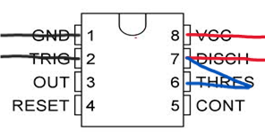
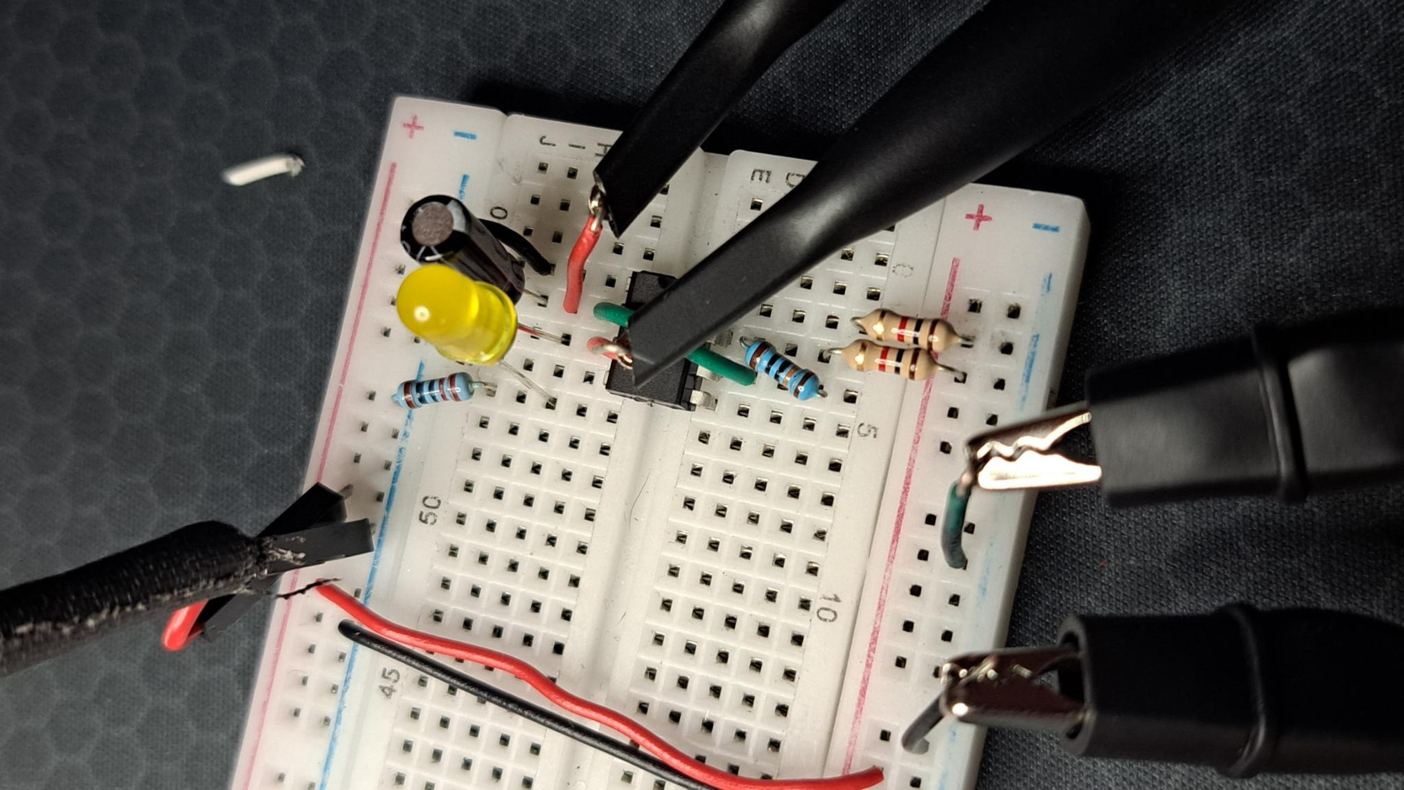
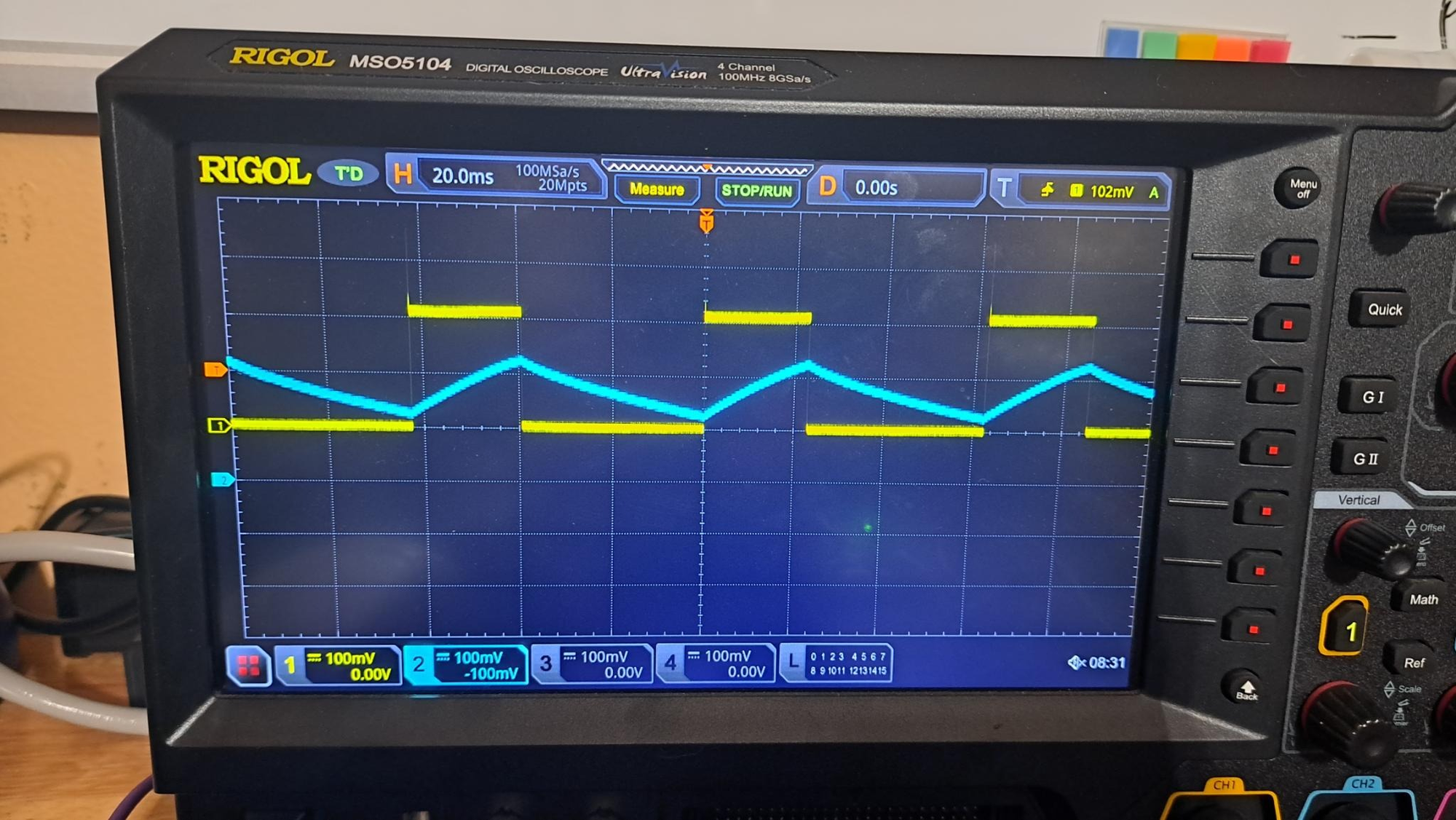
Now moving back to the Oscilloscope, we gonna want use two probes for our purposes this time. We'll start again with the first probe connected through one of the ends to Pin 3 (Output), on the Chip, and the other to Ground.
Attach the second prob to the Junction between Pin 2 and the 1uF, (Micro-Farad), capacitor. This line will read the Charge/Discharge of the capacitor as is Builds up and then empties. As well as connect the other end of the second probe into the Ground line, just like the first.
Figure 13
**Make sure your probes looks something like, or similar to what's shown in the picture's above and below**
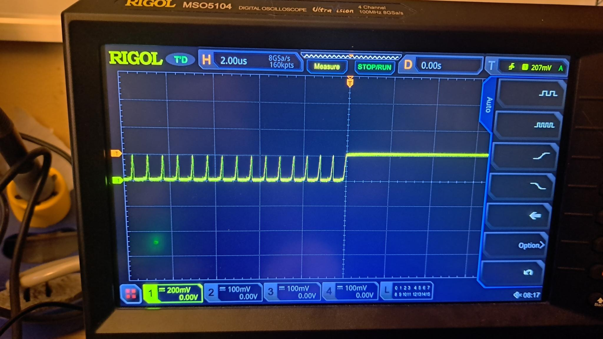
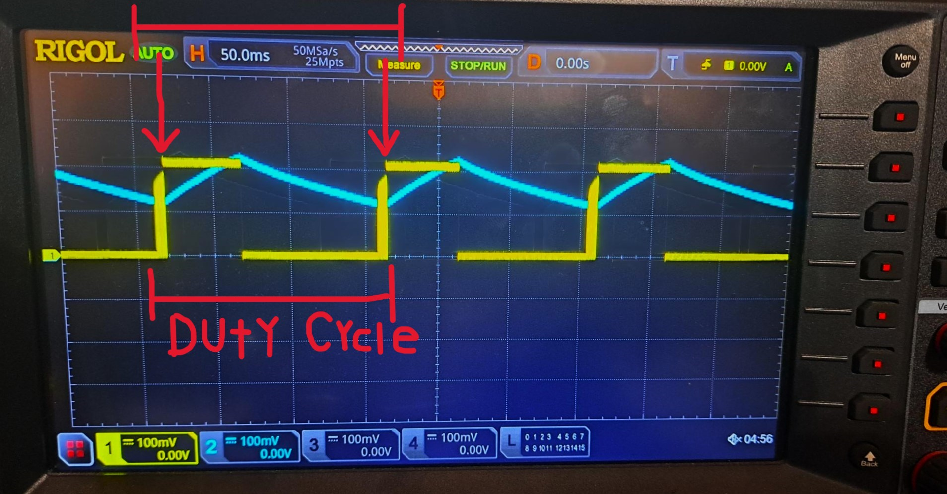
Now power back on your Oscilloscope and take look at the screen. Measuring 100ms ( milli-seconds), in length, The Yellow line, is the Output ( O ), voltage signal coming from Pin 3 on the 555 Timer. Its shaped like a square sign wave just like before.
The Blue line, is the 1uF Capacitor's, charge Increasing and decreasing as the capacitor's voltage fills up all the way to the peak of the Yellow line at 5 Volts, until the capacitor then empties again, We see the slope of the capacitor as it drops down with the signal back to 0.00 Volts again.
Figure 14
(* You may have to adjust the on-screen settings and the scale of sign wave properly like before, but again the Settings/Adjustments on the Oscilloscope may vary from the one used here depending on your make and model *)
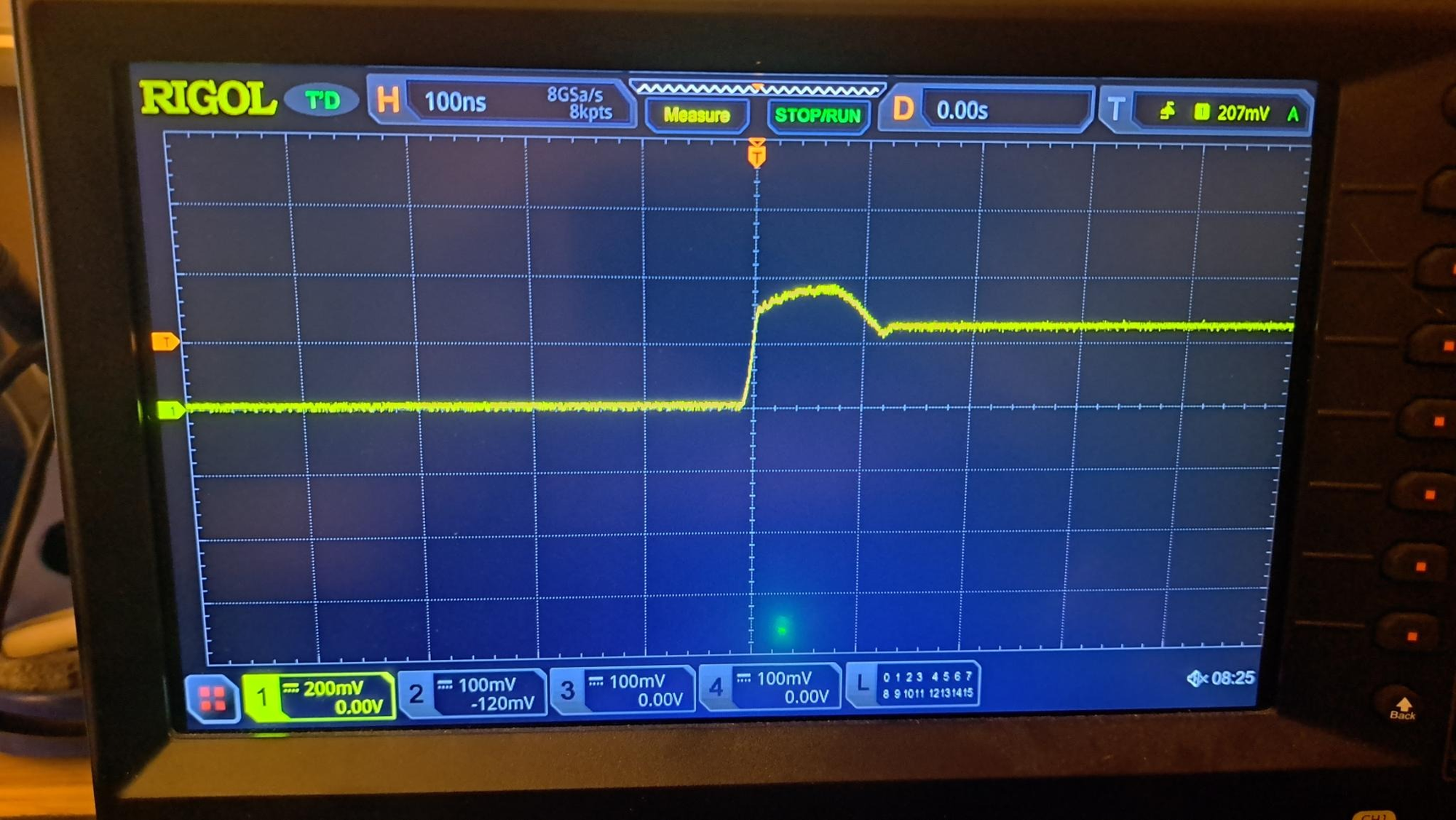
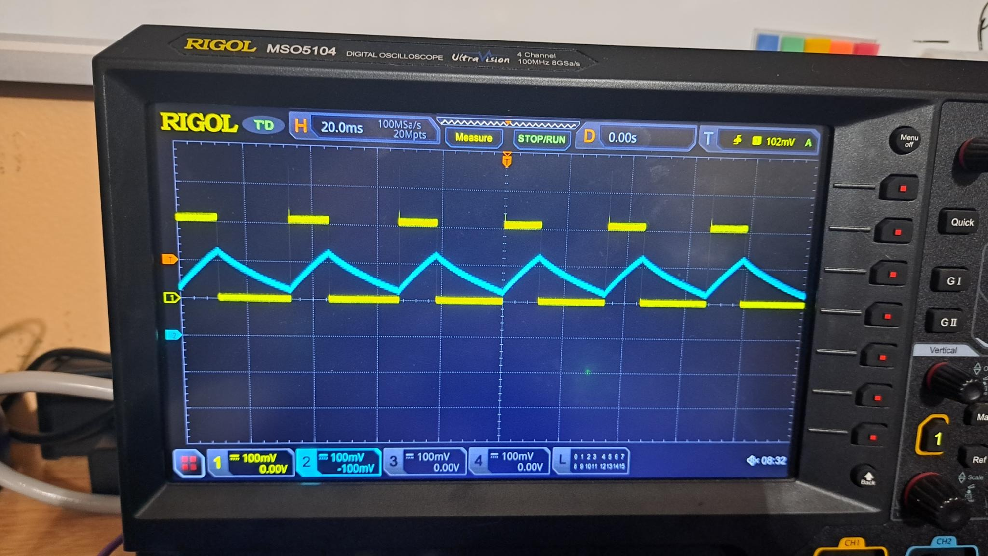
Now if we zoom in to that line right where the voltage peaks, we would see that clean transition from 0.00 Volts, up to 5.00 Volts actually is not so clean.
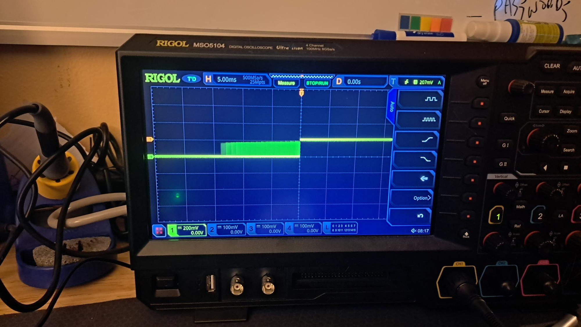
What we end up seeing zooming in even more, evidently, is just a lot of noise. As the signa's oscillation moves up and down, the waves curve also oscillates between the 0.00 and 5.00, Voltage.
We can attempt to smooth out this curve.
Looking at the data sheet, it states that Pin 5 of the 555 Timer, "Controls comparator thresholds, Outputs 2/3 VCC, allows bypass capacitor connection. ", so by putting a 0.1uF Microfarad capacitor connecting Pin 5 to ground on your breadboard, you should be able smooth out the transitions between timings a bit. ( *Adding a second 0.1uF capacitor across the power and ground lines of your breadboard can additionally help with smoothing out the signal's level* )
Strangely, my NE555 Timer's Outputs levels don't seem to be affected by the 0.1uF, Microfarad capacitor on Pin 5, so I've had to connect a capacitor instead, across from the 555 Timer's Power Pin, ( Pin 8 ), directly to Ground through a grey wire.
Now if you've ever looked at an actual 555 Timer on a circuit board, (typically) most of the time, the manufacturer will actually place a capacitor right next to the 555 Timer's power supply. Putting the capacitor closer to the 555 Timer, it'll allow for an even smoother current transition from 0.00 Volts to 5.00. ("For most use cases with 555 Circuits like this one don't actually require that precise of timing.")
So now you should actually start seeing a wave more like this on you screen.
When the circuit starts pulling from the 1uf capacitor on pin 2, initially it actually begins to pull more current than necessary, as we can see this up and down wave as the current begins to level out. (" Honestly It should be way more of and up and down motion as the signal starts to level out back down to 5V's but its actually quite smooth here, not quite sure why but nevertheless" )
We call this the "Duty Cycle", of the 555 Timer. If we go and look at the data sheet for the NE555 Timer, they actually can provide us more information on how to calculate the Duty Cycle of the circuit for your own. As well as what the cycle should end up looking like depending on your model of IC.
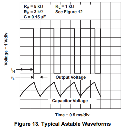
Here the 555 Timer's data sheet ("Figure 13"), shows the NE555's typical waveforms generated during A-Stable operation. The Output High-Level's duration, tᴴ, and Output Low-Level's duration, tᴸ, can be calculated as shown in the formula below.
This Formula used to calculate the total time of the 555 Timer's duty cycle yourself. The main part of this formula to be focused on is:
tᴴ =0.693( Rᴬ + Rᴮ ) C and, tᴸ = 0.693( Rᴮ ) C .
The ( tᴸ ), shown here, the Output Low Level's duration is equal to ( Rᴬ ), the first 1k (Kilo-Ohm) resistor in Pin 7 of the 555 Timer.
( Rᴮ ) is the 100k (Kilo-Ohm), resistor we attached before from Pin 6, to Pin7. ( Fig. 3 )
So if we take the resistance of the second resistor and times it by 2, or 200k (Kilo-Ohms), ( Remember that since the capacitor on the outside 5 volt power line has to go through the 100k resistor twice to discharge through the Discharge Resistor ), then we add the resistance of the first resistor on pin 6, so that's 201k Ohm's total. Then multiply that by the capacitor's capacitance, ( 0.000001 ), or 1uF (Micro-Farads), we'll get 0.201. Now times that by 0.693, ( *The reason for 0.693, is its the manufacturer's coefficient determined based on their own calculations to make finding the time constant for us a bit easier* ), and finally we have our clocks Duty Cycle: 0.139293.
0.139293 should be the total time for the Duty Cycle's, Output Levels High, and Output Levels Low state's time spend ON ( High ) &, OFF ( Low ).
or 0.139 (Milli-Seconds) spent turning ON, then OFF again.
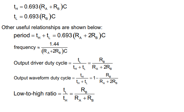
Other formulas are also helpful when performing this type of work, such as:
period = tᴴ + tᴸ =0.693(Rᴬ + 2Rᴮ)C
frequency ~ 1.44 — (Rᴬ +2Rᴮ )C
(Rᴬ + 2Rᴮ)C is just the First resistor (Rᴬ) plus the Second Resistor times 2, (2Rᴮ). which function basically the same as multiplying the 100k Ohm resistor by 2 like we did before. So for this project you can go ahead and ignore the rest of the the formula tables.
Now Something to notice while taking these Oscilloscope measurements, is that the measurements readings on the Oscilloscope's screen horizontally is divided up by 50ms, (Milli-Seconds) and if count those sections up till the duty cycle's Output Levels High, and Output Levels Low state, we read something around 200, 250-ishms milliseconds. Now that's obviously not correct by our calculations we did manually to get 0.139293.
This doesn't seem right, and the answer is quite strange, but makes some sense as to why we're reading this value.
If you take your, (or a), Multi-meter and put both ends of the 1uf, Micro-farad capacitor's legs to the meter, you might actually strangely, end up reading 2uF Micro-farad'(s). ( Mine is somewhere closer to 1.8 uF, Micro-farad but nevertheless. )
I'm not to quite sure the case of why this is, possibly a manufacturing error. Either way the simple fix to this, is to just multiply our clocks cycle's time by x2. So 0.139293, will instead be 0.278586, making our timer's Duty Cycle actually, 0.278 total milliseconds long.
This technique for manually calculating the 555 Timer's Duty cycle yourself can be extremely helpful when working on circuit's requiring extremely precise timing for operations, but for this case its just good to confirm and compare the differences between your own calculations and the measurements you've observed from the oscilloscope itself.
Manually Controlling the Circuit's Signal:
Now one thing that would be useful with this 555 Timer would be some way to control the timings of the signal. This is helpful when creating simple 8-bit computer ram modules, being able to adjust the timing of the output signal based on whatever value you set to it.
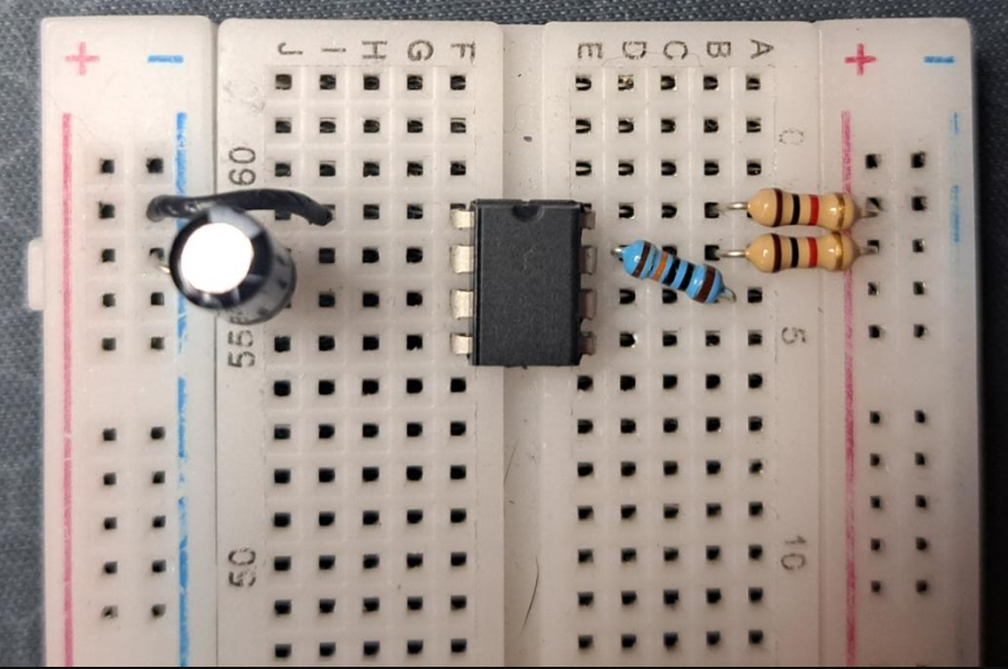
For this we'll use a 1M, (Mega-Ohm) Variable Resistor, placed just above the IC on the breadboard like so:
Once on the board, remove the 100k resistor on the 7th Pin of the 555 Timer, and instead connect a 1k, Resistor through to the pin closest to the top of the Potentiometer. ( I had to really squish my resistor in there since of how small of a space with the capacitor in the way, you're circuit's configuration may have to differ a bit )
As well as, make a wire connection from Pin 6 to the middle pin of the Potentiometer. This will in turn change the Voltage that's coming through the 1uF capacitor, varying between the 1,000 and 0 resistor range. Connect the bottom last pin of the Potentiometer to ground (Black Wire).
Now hook back on the probes like before, and take a look at your oscilloscope.
The Signal's length now should depend on how much you turn the Potentiometer, also changing the spacing between the signal's wave.
*Notice the signal's length will change corresponding with how far you adjust the Variable resisting potentiometer to the left and right*
And with that, you've successfully made your very own 555 Precision Timer circuit using the NE555 Integrated Circuit. As well as read the Output signal coming from that timer using a Digital Oscilloscope. Congratulations!
Conclusion:
In conclusion, this project walks through the process and the concepts of how to successfully hook-up, make, and analyze the typical A-Stable sign wave signal generated us the 'NE555' Integrated Precision Circuit Timer. Created Entirely on a Breadboard and using an Oscilloscope
Thank you for reading, and have a great day!
Matt Clark, @, RedCrowLab LLC.